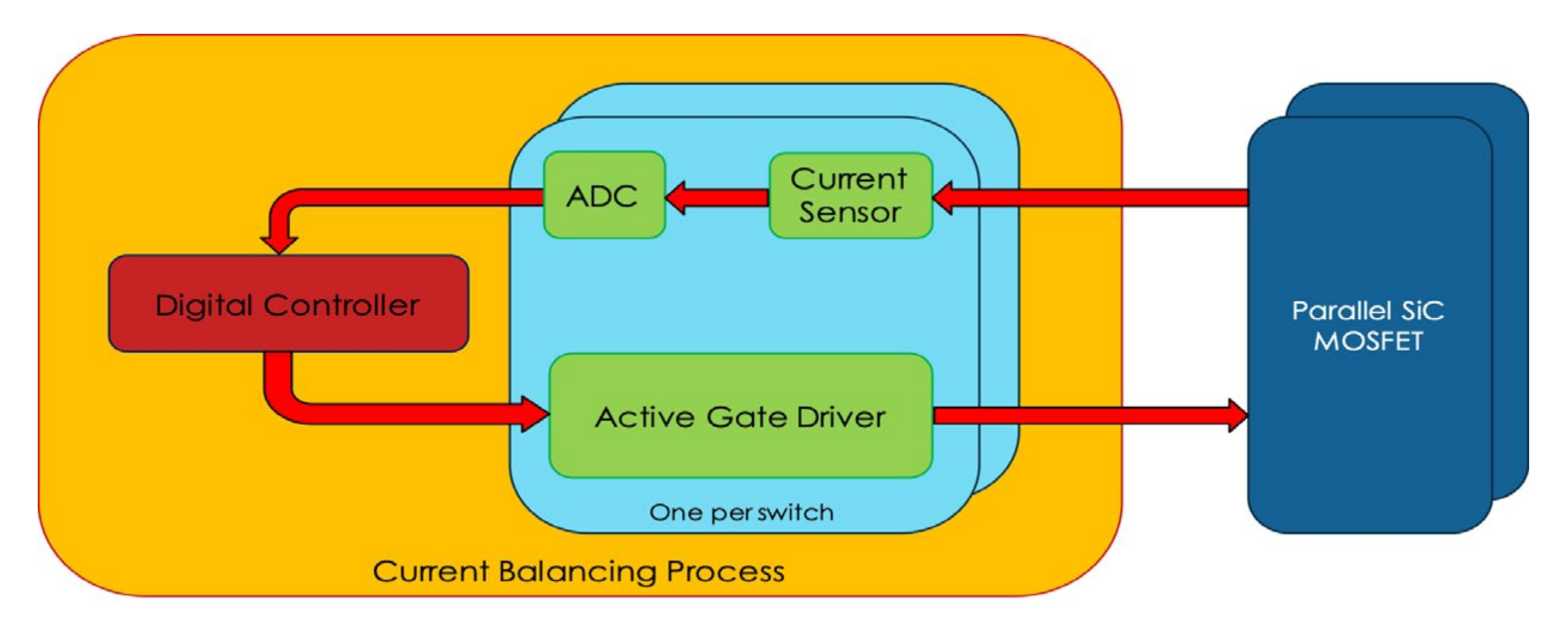
In comparison to silicon, silicon Carbide (SiC) adds power and strength to power converter designs as well as high power density and efficiency (Si). In recent years, it has been observed that the failure-in-time rates of SiC have decreased and are now comparable to those of Si. The degradation of the gate oxide is expected, and this is a concern that limits the widespread use of SiC in military, transportation, and manufacturing applications.
A catastrophic breakdown in silicon carbide-based power converters can be easily avoided by indicating the impending failure, which can be checked by monitoring the silicon carbide MOSFET. However, calculating the gate leakage current from the actual measured gate current is difficult.
The gate current is dominated by the process of charging and discharging transients of the gate capacitor. The inductor introduces second order ringing, which complicates the calculation process.
The introduction of an in-situ method for measuring gate charge is one solution to the aforementioned challenges. The differential voltage across the gate resistance and gate current are proportional to each other, whereas the monitoring circuit in figure 1 tracks the voltage on each silicon carbide device.
Fig. 1: Monitoring Circuit
Aging-Detection
Figure 2 depicts the circuit for detecting SiC MOSFET aging. The goal is to calculate the total amount of charge that has leaked and entered the MOSFET gate during the time period. The sensing circuit calculates the leakage current of the gate by measuring the voltage Vrg across the external gate resistance Rg.
Fig. 2: Aging Detection Circuit
Even in the presence of a degraded MOSFET, there is no leakage in the scenario described for the given figures. The problem is eliminated by the precision rectifier’s measurement of the positive current into the gate. Vs is completely dependent on the operating duty ratio, indicating that the sensing circuit is insufficient for determining the on-state gate leakage current with accuracy.
The reference circuit is shown in Figure 2. It is recommended that the integrator outputs vs and vr be sampled at the same time in order to estimate the gate leakage current independently from sampling time and duty ratio.
Sensing-Circuit
Figure 3 (a) depicts the measured differential voltage Vrg across the gate resistance. For the silicon carbide mosfet experimental setup, a switching frequency of 50kHz and a duty ratio of 0.5 were used as statistics.
Figure 3 (b) depicts the In-Amp output v1, which is designed to produce a unity gain and produce an output waveform that is identical to the differential input. The experimental data was analyzed and waveforms were generated using the data collected. By resetting the healthy silicon carbide mosfet where the output voltage is calibrated, the effect of the switching turn-on transient is eliminated.
Fig. 3: Sensing circuit waveforms.
Reference-Circuit
The gate driver output is directly received by the precision rectifier of the reference circuit. Gr denotes the precision rectifier’s gain, which is the ratio of R3 and R4. It is chosen so that the integrator output does not saturate. Figure 4 (a), (b), and (c) show the vg, v3, and vr waveforms, respectively.
Fig. 4: The reference circuit’s waveforms.
Simulation Results
The following formula can be used to calculate the gate leakage current:
Ig,lk-on = (GsRg /GrVg-on) Vs,cal(Ts)/ Vr(Ts)
The gate driver circuit determines the values of Vg-on and Rg, while the values of Gs and Gr are determined by design and the values of Ig,lk-on, Vs,cal, and Vr are calculated through sampling. The simulation waveforms are depicted in Figure 5. The non-ideal properties of the circuit and components such as op-amp affect the accuracy of the leakage current value, as does the introduction of noise.
Fig. 5: Simulated Waveform
Experimental Setup and Results
The schematic diagram for the gate driver and age detection circuit with 1.7kV SiC MOSFETs and a frequency of 50kHz is shown in Figure 6. The lower side FET is wired to the aging circuit, and an external resistor is connected to draw extra gate current. Figure 7 illustrates the prototype.
The findings show that the voltages Vs and Vr rise over time. The calculation of the gate leakage current is aided by sampling Vs and Vr for different time periods.
Fig. 6: Experimental Setup
Fig. 7: Prototype
Conclusion and Future Work
The gate leakage current is the basis for the technique used to monitor the health of the SiC MOSFETs. The measurement of gate current in a direct manner is complicated by the wide dynamic range and high frequency. The experimental results have validated the expected waveforms.
By utilizing the health monitoring capabilities, the integration of an aging detection circuit and a gate driver can result in a more solid design of the power converter. This approach can be used to estimate the gate current in other power transistor families, such as IGBTs and GaN.


More Stories
5 Ways to Boost Data Security on the Cloud
Apple Black Friday Sales, iPhone 15 Pro rumors, Device Buying Guide
How Businesses Can Overcome Cybersecurity Challenges